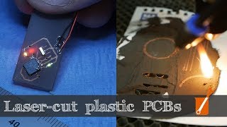
Make plastic printed circuits with a standard laser cutter
Channel: Applied Science
Category: Science & Technology
Tags: circuit boardelectronicsmakingcopper platingtartrateapplied scienceelectroless copperben krasnowkrasnowprototypelpkfpcblaser cutterpcbsplatedplated through holelaserdiylaser definedcopper platedcircuitrycopper circuit
Description: I developed a new chemical process to make double-sided PCBs with a laser cutter, and some common chemicals. This is intended to be used on SLA 3D-printed parts, but may work on many materials. Refs: infohouse.p2ric.org/ref/29/28004.pdf citeseerx.ist.psu.edu/viewdoc/download?doi=10.1.1.527.5817&rep=rep1&type=pdf shodhganga.inflibnet.ac.in/bitstream/10603/195088/3/chapter%202.pdf sci-hub.tw/https://doi.org/10.1016/S0167-577X(03)00424-5 library.nrao.edu/public/memos/chem/CHEM_5.pdf core.ac.uk/download/pdf/48645791.pdf Support Applied Science: patreon.com/AppliedScience